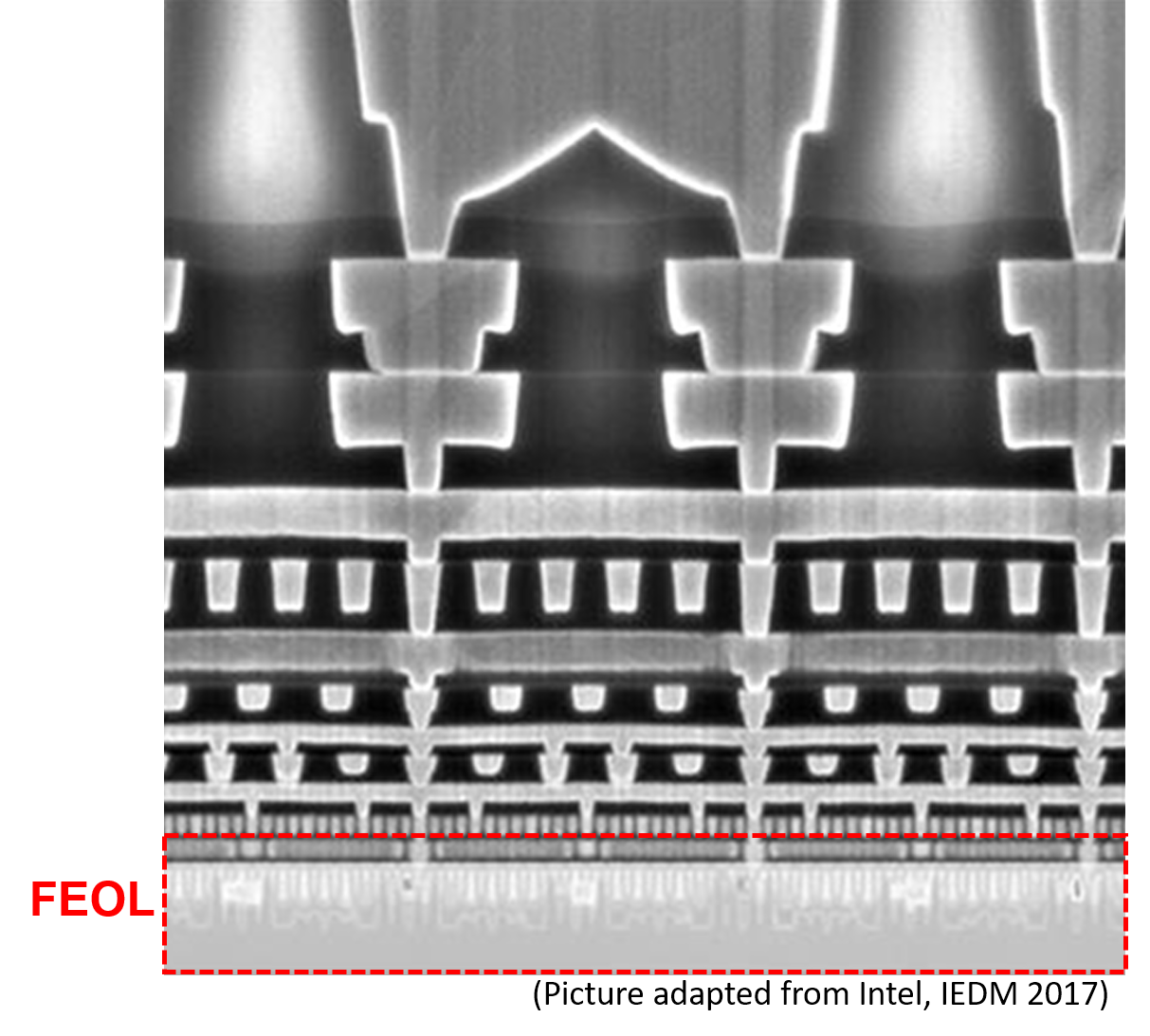
As integration engineers, we are responsible for delivering the 20nm technology node.
To deliver technology successfully, we have to achieve >80% yield, pass qualification,
and meet device performance, etc. Therefore, we had to identify all the issues and gather
information from inline data, eFA, WAT, defect counts, many other tests, to figure out all
the issue root causes. We highlighted issues to module teams to ask for resources to solve them.
As integration is the center of the technology platform, we collaborated with 10+ cross-
functional teams and our judgement was crucial to the success of the technology.
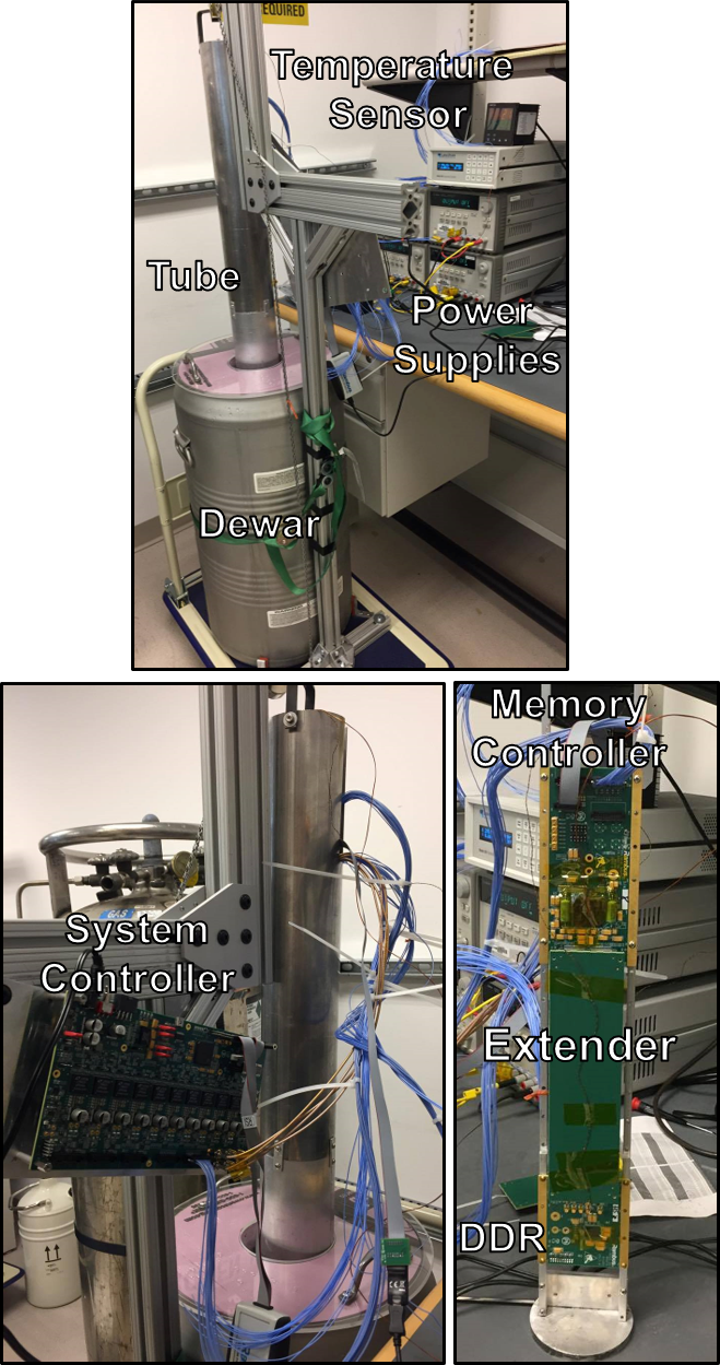
“Cool” Memory Retention Testing
DRAM is a promising memory option for quantum computing as it has high retention at low
temperatures. The task assigned to me was to determine the exact retention of DRAM at cryogenic
temperatures. In order to do so, I worked with teams that designed PCB boards for DDR2/DDR3
in North Carolina to figure out the power requirement of the PCB boards. Afterwards, I set up
the testing environment in Sunnyvale for PCB boards and developed software programs for
retention testing. I investigated the retention failure mechanism by carefully characterized
temperature dependency and writing different patterns. In the end, we determined that GIDL
ultimately limited the DRAM retention time and that peripheral circuits need to be customized
for low temperature operation.