The goal of my PhD research was improving the computing speed through the innovation of Two dimensional (2D) material electronic.
2D materials have an intrinsic layered atomic structure with only weak vdW force between layers. Such feature makes
2D materials promising for transistor scaling, vertical 3D integration, ultra-thin heterojunction and many other applications.
During my PhD, I completed three projects that nicely covered these different perspectives of using 2D material for electronic devices.
The computing speed is not limited by the single device performance but the bandwidth between on chip logic and
off chip memory, which is called the “memory wall”. 3D stacking memory on logic would be the most efficient solution
for breaking this wall and 2D materials are promising for 3D stacking due to their low temperature processing. To
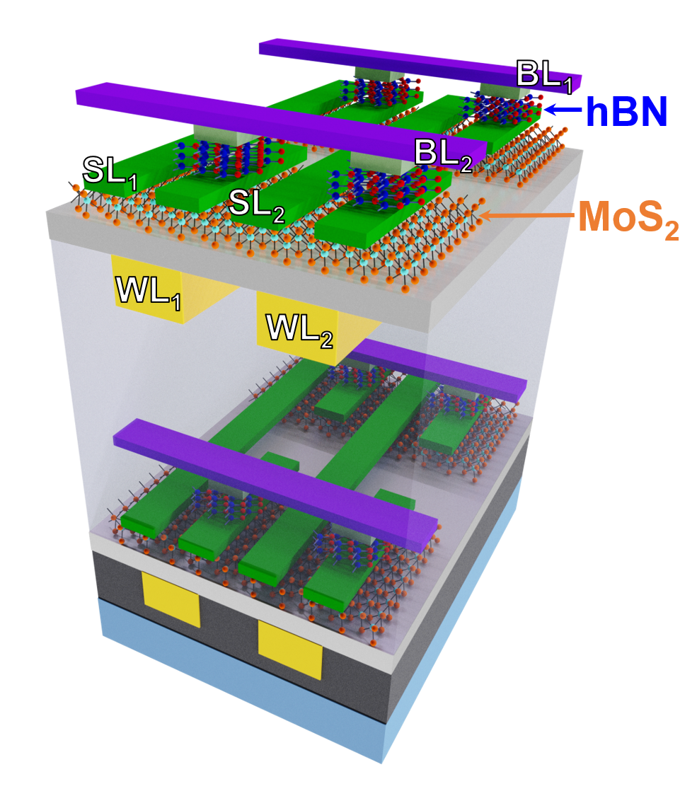
demonstrate this promise, I designed and fabricated a novel 3D monolithic memory cell, integrating MoS2 FETs and RRAM
for high density non-volatile memory.
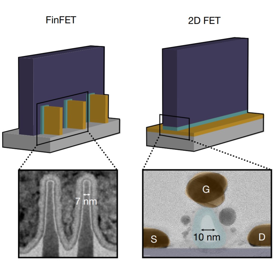
Two-dimensional scaling of silicon transistors is coming to an end. Future computing system improvements will most
likely rely on an integration of novel materials and processes. 2D materials have an intrinsic layered structure
and a wide range of properties that can be used for various computing applications. This review paper catalogues the
meaningful progress we have made over the past few years and the direction to move forward to. I contributed to the
section on 2D materials for memory and interconnect technologies.
Ultra-thin Memory Selectors
In this era of data-driven applications, memory technology has become increasingly important.
In order to achieve a high density memory array, two-terminal selectors are necessary. However, commonly used
threshold-type selectors suffer from many issues originated from their ion/atom motion-based mechanism.
Non-threshold type selectors are based on a reliable tunneling.
However, non-threshold type selectors are made of oxide layers,
therefore the traps in oxide limit the endurance and current drive.
2D materials are the best candidates to replace oxide.
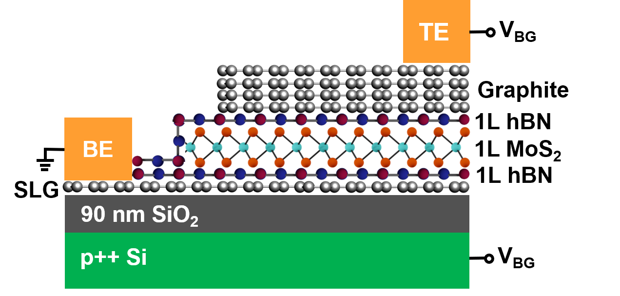
In this work, I developed the first ultra-thin (≤ 3 monolayers) 2D
material memory selector. This work is the foundation for using 2D materials for high endurance non-volatile memory system.
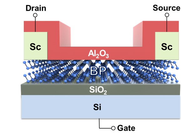
Black phosphorus (BP) is an air sensitive 2D material (and one kind of thin film material) with a theoretically superior
mobility than other 2D semiconducting materials. Most research has focused on p-type transistor, however, for CMOS, fabricating
p-type and n-type transistors on the same material is necessary. In this research, I developed a novel BP transistor
with Scandium as source/drain contacts and achieved a record high on-current of n-type BP FET. I had to overcome several
fabrication challenges, such as air sensitivity, meaning many late nights.